From 27C3 public wiki
Embedded Analysis
This document covers embedded analysis techniques and tools. It can be used as a guide during our talk at the 27c3 or as a reference thereafter. This talk was meant to introduce software analysts to hardware, giving them the tools and knowledge require and hopefully convincing them that it is easy and fun. We will release tools for finding debug interfaces, dumping memory and tracing PCBs. We will go into techniques for redocumenting undocumented interfaces and looking for the human hand in the aesthetics of the target. Please feel free to contribute and edit religiously.
Development of the tools herein was supported in-part by Recurity Labs (RS232enum, JTAGenum, FLASH Dumper), Christopher Tarnovsky (FLASH Dumper) and SRLabs (DePCB).
Contents |
Introduction
All non-trivial abstractions to some degree are leaky -- Joel on Software
Joel was speaking about software development but this rule can also be applied to hardware, especially embedded, security. Consider the abstraction layers between different fields of development that go into making a single device.
- Chip/ASIC designers
- PCB/layout designers
- Embedded software developers
Each might require different debug interfaces. Each also bring their own nuances and common design practices that influence the physical layout and look of the device. The aesthetics give clues as to interesting demarcation points to look at. For example consider a security specification that requires a certain secure chip be placed under a layer of epoxy. The purpose of the epoxy is to make the pins of the chip difficult to probe and to make it difficult to remove. However, in the following example you see a chip placed under epoxy but whose contacts are exposed on the bottom side of the PCB, making this measure near-moot.
top 
 bottom
Important note about voltage levels
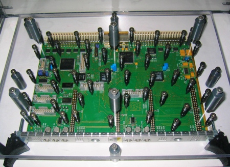
Many of the tools discussed herein use a microcontroller to communicate with the targets pins. It is important that both use compatible voltage levels. Arduino boards use 5v by default. Some are switchable and the others can be modified by installing a voltage regulator on the VCC line or USB cable (example voltage 3.3v regulator installed on Teensy++ board). Resistors in series can also be used for each line. Other methods are discussed here.
Serial
If you think about serial and embedded devices the first thing that comes to mind is probably a serial console on home routers. Such consoles might provide means to configure and debug the device. But serial is used for much more. You will find serial used between a baseband processor and the primary CPU to send AT modem commands. It might be used to programming the memory of a micro-controller or DSP, and much more. Checking the voltage level of all possible target pins, pads and vias can help reduce the set. Serial will be commonly found at +/- 3.3v, 5v and sometimes +/- 12v. 3.3v is a very common TTL level found in embedded electronics so this characteristic in itself does not indicate serial.
Serial Scanning

RS232enum (code) is a Arduino based program (see Arduino Appendix) that can be used to scan and find serial on 30+ pins, vias (through-holes) and pads. Load the sketch onto your arduino and then open a serial console at 115200 buad. There are 3 basic scans that will be run:
Passive Parallel
Passively monitor all attached pins/vias/pads for 4 seconds. If the state (1 or 0) changes print "active" pins to the console. Note: active pins might indicate an RX pin or it might indicate some other interface. Example output shows activity but not enough to indicate serial:
-> passive_parallel_scan(4000000)
   PIN35=1  PIN27=1  PIN29=1  PIN31=0  PIN33=1  PIN33=0  PIN33=1  PIN33=0
   PIN33=1  PIN33=0
Active Parallel
For each pin, choose 1 as the TX pin and send a wakeup signal (such as a carriage return, \n) at various baudrates. Pins that respond indicate both the RX and TX serial pin. Example output showing potential serial activity when a 0x0A, \n, is sent (baud 115200, TX PIN33, RX PIN27):
-> active_parallel_scan(4000000)
   baud: 9600
   0x0A -> PIN35:	PIN33=1
   0x0A -> PIN27:	PIN40=1
   0x0A -> PIN37:	PIN27=0  PIN40=0  PIN27=1
   [...]
   baud: 38400
   0x0A -> PIN35:	PIN40=0
   0x41 -> PIN35:	PIN40=0
   0x41 -> PIN27:	PIN40=1
   0x41 -> PIN37:	PIN40=0  PIN27=1
   [...]
   baud: 115200
   0x0A -> PIN33:	PIN27=1  PIN27=0  PIN40=1  PIN27=1  PIN27=0  PIN27=1  PIN27=0  PIN27=1
   PIN27=0  PIN27=1  PIN27=0  PIN27=1  PIN27=0  PIN27=1  PIN27=0  PIN27=1  PIN27=0  PIN27=1
   PIN27=0  PIN27=1  PIN27=0  PIN27=1  PIN27=0  PIN27=1  PIN27=0  PIN27=1  PIN27=0  PIN27=1
   PIN27=0  PIN27=1  PIN27=0  PIN27=1  PIN27=0  PIN27=1  PIN27=0  PIN27=1  PIN27=0  PIN27=1
   PIN27=0  PIN27=1  PIN27=0  PIN27=1  PIN27=0  PIN27=1  PIN27=0  PIN27=1  PIN27=0  PIN27=1
   PIN27=0  PIN27=1  PIN27=0  PIN27=1  PIN27=0  PIN27=1  PIN27=0  PIN27=1  PIN27=0  PIN27=1
   PIN27=0  PIN27=1  PIN27=0  PIN27=1  PIN27=0  PIN27=1  PIN27=0  PIN27=1  PIN27=0  PIN27=1
   PIN27=0  PIN27=1  PIN27=0  PIN27=1  PIN27=0  PIN27=1  PIN27=0  PIN27=1  PIN27=0  PIN27=1
   PIN27=0  PIN27=1  PIN27=0  PIN27=1  PIN27=0  PIN27=1  PIN27=0  PIN27=1  PIN27=0  PIN27=1
   [...]
Active Per-Pin
This is similar to Active Parallel except that each RX pin is checked individually. Example output shows likely serial (TX=PIN33, RX=PIN27):
-> active_per_pin_scan(4000000)
   tx:PIN35 rx:PIN27 baud:9600
   0x0A -> PIN35:	PIN27=1  PIN27=0 PIN27=1  PIN27=0  PIN27=1  PIN27=0  PIN27=1 PIN27=0
   [...]
When an active pin(s) is found, connect to a serial cable to explore further. It is useful to have an RS232 to USB breakout cable or board available such as those sold at tinkersoup (in Berlin, 5v and 3.3v compatible), sparkfun and others.
JTAG
JTAG can be used to debug running software, check the health of solder joints, check connectivity between IC's and checking or setting the state of pins on a JTAG enabled IC. JTAG IC's can be chained together so that one bus (set of pins) can be used for all of them. There are 4 pins required. TDI (input) TDO (output) TMS (state machine) TCK (clock). TDI and TMS require a pull-up resister between 1k and 10k. More commonly 4.7k is used and if you find such resistors on your board these and neighboring contact points are good places to start scanning.
How it works
 The JTAG registers and lines (pins) |
 Input line |
 Output line |
 Clock line |
 State machine line |
 Provided the ID register is the default on reset we only need to toggle TCK and read the output on TDI |
 The Boundary-Scan register can be used to check the state of pins and internal registers (defined in the target chips BSDL file) |
 If we provide input on TDI we can also set the state of pins and internal registers of the boundary scan, in addition to reading current state |
 The TMS line is important for being able to switch between different registers. |
 Hence, the reasoning behind the 4 JTAG lines |
 Several JTAG enabled chips can be chained together on the same lines. In this example the first is set to access the Boundary Scan register, and the second is set in BYPASS mode |
JTAG Scanning

JTAGenum (code, further documentation) can be used to find JTAG amongst a set of 30+ pins, vias or pads. The standard JTAG instructions (IDCODE, BYPASS) are used to scan for pins.
BYPASS Scan
For each of the pins in the target set a random pattern is clocked through TDI (using TCK to clock). If the pattern is found on the potential TDO pin this indicates JTAG. Example output:
> s
================================
Starting scan for pattern:0110011101001101101000010111001001
active  tck:PIN_1 tms:PIN_4 tdo:PIN_3 tdi:PIN_5 ntrst:PIN_2 bits toggled:12
FOUND!  tck:PIN_1 tms:PIN_5 tdo:PIN_3 tdi:PIN_6 ntrst:PIN_2 IR length: 5
active  tck:PIN_1 tms:PIN_5 tdo:PIN_3 tdi:PIN_7 ntrst:PIN_2 bits toggled:37
active  tck:PIN_1 tms:PIN_6 tdo:PIN_3 tdi:PIN_5 ntrst:PIN_2 bits toggled:12
active  tck:PIN_1 tms:PIN_7 tdo:PIN_3 tdi:PIN_5 ntrst:PIN_2 bits toggled:12
active  tck:PIN_1 tms:PIN_8 tdo:PIN_3 tdi:PIN_5 ntrst:PIN_2 bits toggled:12
active  tck:PIN_1 tms:PIN_9 tdo:PIN_3 tdi:PIN_5 ntrst:PIN_2 bits toggled:12
active  tck:PIN_1 tms:PIN_10 tdo:PIN_3 tdi:PIN_5 ntrst:PIN_2 bits toggled:12
IDCODE Scan
Assuming the IDCODE instruction is the default Data Register, for each possible pin combination shift out the register. The example shows the IDCODE for an LPC chip on the output:
> i
================================
Starting scan for IDCODE...
tck: PIN_5 tms: PIN_6 tdo: PIN_1 tdi: PIN_3     FFFFFFFF
tck: PIN_5 tms: PIN_6 tdo: PIN_3 tdi: PIN_1     FFFFFFFF
tck: PIN_1 tms: PIN_5 tdo: PIN_3 tdi: PIN_6     4F1F0F0F
[...]
Once the JTAG pins are found OpenOCD or other On-Chip-Debugging software that supports the target architecture can be used to debug software, check pin state or dump memory.
fyi, sometimes JTAG contacts can be found on the edge of chips:
 (src)
(src)
Enumerating Instructions
At the 26c3 Felix Domke "tmbinc" describe how to use telepathic examination of the Instruction Register to determine higher level JTAG functionality (lecture video, paper/cache). In his case he used this to find an undocumented bus. JTAGenum provides some basic functionality for enumerating the Instruction Register. This is not a passive technique. In the source repository you will also find OpenOCD scripts to enumerate instructions.
FLASH Dumping
FLASH memory come in various forms. Some support a CFI interface, others have a proprietary and others use Parallel. Parallel in a simple interface where the address is sent across a series of pins and the data is returned across separate set of pins. The Parallel Flash Dumper code loaded onto an arduino is used to dump the memory to the serial console at 115200 baud.
The following breadboard layout shows (made with Fritzing, sketch/source) an ardiuno board connected to a FLASH chip with 23 address pins and 16 data pins. Shift registers are used to take one line of the arduino and turn it into 23 address lines (serial to parallel shift registers) and take the 16 data lines and convert it back into bytes sent across another arduino line (parallel to serial shift registers). To desolder and remove a TSOP FLASH chip from your target see this video.


The code might need to be modified depending on the order and specifics of the state pins for your target FLASH chip. The following image shows the order and state for a Spansion FLASH chip. The minimum timing specifications (tRC, tACC, etc) are not important. What is important to note is that, in this example, RESET# and WE# are pulled high first, the the address is sent, then CE# and OE# are pulled low, then data is read.

You will also need to know where the address, data and state pins are on the chip. Likewise this is found in the datasheet.

Redocumenting Undocumented Interfaces
More often then not documentation will be hard to obtain. If after searching datasheetarchive, pudn 52rd and google, you still cannot find your datasheet you might be able to obtain a pinmap using electrical analysis. Looking at the resistance between Vcc and Ground you might notice patterns that indicate address and data pins. Here is the resistance between ground and the pins of an undocumented FLASH chip.

Comparing this to the ONFI NAND FLASH specifications, which defines footprints for common FLASH interfaces, we can piece together the proper pin map. The following shows our pattern compared with the 48 pin TSOP 16 bit ONFI standard:

The Vcc and GND pins might be a match but the IO pins clearly are not. However, compare our pattern to the 16 bit specification:


A near complete match. The VSP3 pin in the lower left is a "Vendor Specific Pin". This pin is optional so that it shows up on our board as nc (not connected) is not surprising.
This technique can be used for memory and potentially other IC's as well. In addition to documents such as the ONFI standard you could also compare the chip to other chips from the same vendor, that have the same footprint.
DePCB Analysis
DePCB is a PCB tracing tool. This is directly inspired by degate, the IC Logic RE software, from Martin Schobert. In its current state this assists in manually tracing PCBs. In addition to reverse engineering the PCB this can also be useful to document specific interfaces you are examining. In the near future it will support auto-tracing using both visual analysis and heat signatures from thermal imaging.
To begin you will need images of each layer of the PCB. We will use a simple 2 layered board as an example. The images will need to be aligned and you will find a tool in the repository to assist with this task. Once aligned open in DePCB. The following shows an example trace. Selecting a via/pin/trace will show you all of the other points that this trace connects to. In this example the 0v line was selected for examination.
 top
top bottom
The above took under 10 minutes to map by hand.
Aesthetics, The Human Abstraction Layer
Additional clues can be found with a discerning eye toward the aesthetics of the layout and seemingly quaint elements of the target. Particular attention should be giving to the style and cluster of pads/vias/pins and markings for missing connections. For instance, pads which have slight indentations perhaps indicate that they were used in a bed of nails tester commonly used for automated quality assurance testing during manufacturing (component placement). If a small set of vias have solder left on them while others do not it is a indication that 1. they are related to each other 2. they are likely used for some form of testing or debugging.
 RJ45 connector |
 FLASH socket |
 SD slot |
 Non-ground and ground pads. Check for slight indentations that might indicate they were used for testing. |
 Large cluster of ground vias typically for RF areas of PCB |
Hidden vias. If you scrape away the enamel you can use them |
 Alignment markings for automated placement machines |
Appendix
Arduino
Arduino is a prototyping platform. It is commonly used by art students and your children. The platform uses a AVR (some clones use a PIC) microcontroller and provides a simple IDE. Code is commonly coded in C and is well documented.
Additional JTAG Scanning Tools
- JTAG Finder -- the microcontroller provides a pin protocol/interface to a C client running on the PC which does the actual scanning logic. This was one of the first (if not the) JTAG scanner. It trades simplicity of code and protocol for efficiency and speed.
- JRev -- Not meant for scanning pins to find JTAG. It does however implement some logic not in any of the JTAG scanners mentioned here. In particular, support for chain mapping and perhaps others I’m missing.
- Arduinull -- The first simplified scanner running all in the microcontroller.
- Additionally Jal2 and Zoobab have written their branches of JTAGenum. I will try to merge their features to the JTAGenum branch as quickly as possible but if you run into problems or for general curiosity you can check their code.
Additional Memory Access Tools
- Flashrom provide code for interfacing with various memory types. They include excellent documentation and have a growing community.