Embedded Analysis

This document covers embedded analysis techniques and tools. This is a resurrection of the Embedded Analysis node from the 27c3 with few new techniques and observations added. Please feel free to contribute and edit religiously. The document is sectioned into finding Serial and JTAG debug interfaces which provides general techniques that may be modified to find additional interfaces, examining the aesthetics of the target for clues that indicate points to look for interfaces or how to narrow the search space and dumping memory.
Introduction
All non-trivial abstractions to some degree are leaky -- Joel on Software
Joel was speaking about software development but this rule can also be applied to hardware, especially embedded, security. Consider the abstraction layers between different fields of development that go into making a single device.
- Chip/ASIC designers
- PCB/layout designers
- Embedded software developers
Each might require different debug interfaces. Each also bring their own nuances and common design practices that influence the physical layout and look of the device. The aesthetics give clues as to interesting demarcation points to look at. For example consider a security specification that requires a certain secure chip be placed under a layer of epoxy. The purpose of the epoxy is to make the pins of the chip difficult to probe and to make it difficult to remove. However, in the following example you see a chip placed under epoxy but whose contacts are exposed on the bottom side of the PCB, making this measure near-moot.
| Top | 
|

|
Bottom |
Debug Interfaces

Voltage Levels
Many of the tools and techniques discussed herein use a microcontroller to communicate with a targets pins. It is important that both (microcontroller and target) use compatible voltage levels. For example, if the tool you choose is arduino based these are typically working at 5v with some offering 3.3v. If the target interface you are searching for or the target memory chip you are dumping operates at 1.8v you will need to place voltage shifters inbetween your tool and target pins. Options for voltage compatibility are discussed in the Voltage Appendix in greater detail.
Serial
If you think about serial and embedded devices the first thing that comes to mind is probably a serial console on home routers. Such consoles might provide means to configure and debug the device. But serial is used for much more. You will find serial used between a baseband processor and the primary CPU to send AT modem commands. It might be used to programming the memory of a micro-controller or DSP, and much more.
Serial Scanning

RS232enum (code) is a Arduino based program that can be used to scan and find serial on 30+ pins, vias (through-holes) and pads. First you should determine the set of pins to scan. Checking the voltage level of all possible target pins, pads and vias can help reduce the set. Serial will be commonly found at +/- 3.3v, 5v and sometimes +/- 12v. 3.3v is a very common TTL level found in embedded electronics so this characteristic in itself does not indicate serial. Connect your Arduino to the target pins and load the sketch onto your arduino and then open a serial console at 115200 buad.
There are 3 basic scans that will be run:
Passive Parallel
Passively monitor all attached pins/vias/pads for 4 seconds. If the state (1 or 0) changes print "active" pins to the console. Note: active pins might indicate an RX pin or it might indicate some other interface. Example output shows activity but not enough to indicate serial:
-> passive_parallel_scan(4000000)
   PIN35=1  PIN27=1  PIN29=1  PIN31=0  PIN33=1  PIN33=0  PIN33=1  PIN33=0
   PIN33=1  PIN33=0
Active Parallel
For each pin, choose 1 as the TX pin and send a wakeup signal (such as a carriage return, \n) at various baudrates. Pins that respond indicate both the RX and TX serial pin. Example output showing potential serial activity when a 0x0A, \n, is sent (baud 115200, TX PIN33, RX PIN27):
-> active_parallel_scan(4000000)
   baud: 9600
   0x0A -> PIN35:	PIN33=1
   0x0A -> PIN27:	PIN40=1
   0x0A -> PIN37:	PIN27=0  PIN40=0  PIN27=1
   [...]
   baud: 38400
   0x0A -> PIN35:	PIN40=0
   0x41 -> PIN35:	PIN40=0
   0x41 -> PIN27:	PIN40=1
   0x41 -> PIN37:	PIN40=0  PIN27=1
   [...]
   baud: 115200
   0x0A -> PIN33:	PIN27=1  PIN27=0  PIN40=1  PIN27=1  PIN27=0  PIN27=1  PIN27=0  PIN27=1
   PIN27=0  PIN27=1  PIN27=0  PIN27=1  PIN27=0  PIN27=1  PIN27=0  PIN27=1  PIN27=0  PIN27=1
   PIN27=0  PIN27=1  PIN27=0  PIN27=1  PIN27=0  PIN27=1  PIN27=0  PIN27=1  PIN27=0  PIN27=1
   PIN27=0  PIN27=1  PIN27=0  PIN27=1  PIN27=0  PIN27=1  PIN27=0  PIN27=1  PIN27=0  PIN27=1
   PIN27=0  PIN27=1  PIN27=0  PIN27=1  PIN27=0  PIN27=1  PIN27=0  PIN27=1  PIN27=0  PIN27=1
   PIN27=0  PIN27=1  PIN27=0  PIN27=1  PIN27=0  PIN27=1  PIN27=0  PIN27=1  PIN27=0  PIN27=1
   PIN27=0  PIN27=1  PIN27=0  PIN27=1  PIN27=0  PIN27=1  PIN27=0  PIN27=1  PIN27=0  PIN27=1
   PIN27=0  PIN27=1  PIN27=0  PIN27=1  PIN27=0  PIN27=1  PIN27=0  PIN27=1  PIN27=0  PIN27=1
   PIN27=0  PIN27=1  PIN27=0  PIN27=1  PIN27=0  PIN27=1  PIN27=0  PIN27=1  PIN27=0  PIN27=1
   [...]
Active Per-Pin
This is similar to Active Parallel except that each RX pin is checked individually. Example output shows likely serial (TX=PIN33, RX=PIN27):
-> active_per_pin_scan(4000000)
   tx:PIN35 rx:PIN27 baud:9600
   0x0A -> PIN35:	PIN27=1  PIN27=0 PIN27=1  PIN27=0  PIN27=1  PIN27=0  PIN27=1 PIN27=0
   [...]
When an active pin(s) is found, connect to a serial cable to explore further. It is useful to have an RS232 to USB breakout cable or board available such as those sold at tinkersoup (in Berlin, 5v and 3.3v compatible), sparkfun and others.
JTAG

JTAG can be used to debug running software, check the health of solder joints, check connectivity between IC's and checking or setting the state of pins on a JTAG enabled IC. JTAG IC's can be chained together so that one bus (set of pins) can be used for all of them. There are 4 pins required. TDI (input) TDO (output) TMS (state machine) TCK (clock). TDI and TMS require a pull-up resister between 1k and 10k. More commonly 4.7k is used and if you find such resistors on your board these and neighboring contact points are good places to start scanning.
How it works
JTAG has 4 required lines. TMS, TCK, TDI, TDO. A 5th TRST is optional. JTAG has a state machine called the TAP. The JTAG TAP has very simple logic that controlls what "register" is active between TDI and TDO (input/output). The JTAG spec defines that by default the IDCODE or BYPASS register will be between input and output. The TCK/clock line shifts bits out of the current register like a shift register or FIFO buffer. To change the register between TDI and TDO the TMS pin is used. The TMS pin controls the TAP. Finally the optional TRST line resets the TAP when toggled.
- JTAG
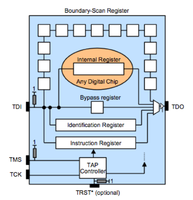
The JTAG registers and lines (pins)
Input line
Output line
Clock line
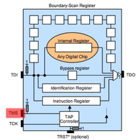
State machine line
Provided the ID register (IDCODE) is the default on reset we only need to toggle TCK and read the output on TDO
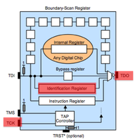
The Boundary-Scan register can be used to check the state of pins and internal registers (defined in the target chips BSDL file)
If we provide input on TDI we can also set the state of pins and internal registers of the boundary scan, in addition to reading current state
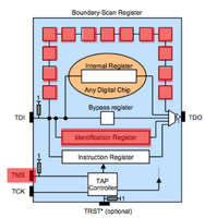
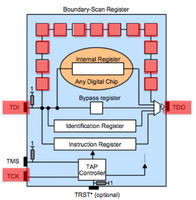
The TMS line is important for being able to switch between different registers.
Hence, the reasoning behind the 4 JTAG lines
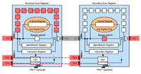
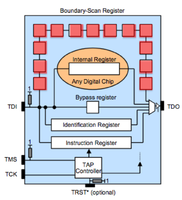
Several JTAG enabled chips can be chained together on the same lines. In this example the first is set to access the Boundary Scan register, and the second is set in BYPASS mode


JTAG Scanning

Scanning Tools
| Tool | Links | Platform | Pin max | Voltages | Note |
|---|---|---|---|---|---|
| JTAGenum | code/docs | Arduino | 13 to 46 | 5v, 3.3v | Dumb and simple. Number of pins dependent on Arduino (Teensy++ for 46). Requires voltage shifting for 1.8v or lower targets. see Voltage Appendix for voltage level shift configurations |
| JTAGulator | code/docs | Parallax | 21 | 1.2v, 1.8v, 2.5, 3.3v | Board is designed for this task and provides support for low voltages without requiring voltage shifters |
| JTAG Finder | code/docs | AVR microcontroller | 13 to 46 | 5v, 3.3v | This was one of the first (if not the) JTAG scanners. People that don't care for Arduino may prefer this solution. Same voltage considerations required as with JTAGEnum. |
JTAG Scanning By Hand
Apart from the default JTAG states that assist in animated scanning electrical requirements for the pins can be used to determine the pins by hand, at best, or at least help determine which pins are likely targets or reducing the set that need to be scanned. Therefor understanding how to find JTAG by hand can also assist in automated scan setup.
Certain JTAG pins must have a default HIGH or LOW state. This is important so that if nothing is happening the JTAG TAP (the state machine) is not jumping around and is instead in the reset state. For example if the TMS pin that determines the state of the JTAG TAP and the TDI and TCK pins are all floating somewhere between HIGH and LOW there is a slight chance that the chip could be inadvertently placed into a state that interrupts the normal operation of the system. To avoid this pins are set into a default state which is facilitated using a pull up or pull down resister to the pins line (pull up means resistor connected to pin and Vcc, pull down means resistor connected to pin and ground). Nearly all specifications recommend using resistors between 1k and 10k with many using 4.7k. The common pullup/pull down recommendations are given below (based on ARM recommendations).
- TCK - pull down LOW (recommended)
- TDI - pull up HIGH (recommended)
- TDO - pull up HIGH (recommended)
- TMS - pull up HIGH (required)
- TRST (optional) - pull up HIGH (required)
You can measure if a pin has a pull down by checking the level of resistance (using multimeter) between a target pin and ground. Ground is common and can be found on metallic plates over chips or even the metal of the devices case. To determine pull up resistance you will need to determine the Vcc line of the chip. In fact you may need to find the Vcc Vref line typically found amongst your target set. This sounds harder than it is.
To find the Vref line you will want to find all the pins of your target set that are in the default HIGH state. What voltage is high? 3.3v and 1.8v are decent assumptions. As a rule of thumb though the HIGH voltage will have at least 3 pins in this state as 3 of the JTAG lines are required to be in this state. Including the Vref pin 4 in HIGH state are required. To find the Vref pin choose on pin as the Vref candidate from the set of HIGH pins and measure the resistance between it and the other pins. Do this for each candidate. Vref will be the pin where the other pins in the set hold a common resistance value to it of range between 1k to 10k.
In the process of determining the Vref pin you will now also know which pins could be either TDI, TMS or TMS. Later we will use what we understand of JTAG's default states (IDCODE or BYPASS) to define them more accurately but for now lets move to finding the TCK pin. To find the TCK pin measure the resistence to ground of all pins at or near 0v during normal device operation. Ideally you will find one with a value between 1k and 10k. If not at least you have already likely thrown away many false candidates and reduced your brute force space.
To "find" JTAG now we can use a common JTAG cable and connect only the required lines based that are determined by which default TAP state (IDCODE or BYPASS) we are testing first. Assuming the chip is in the IDCODE state, meaning the IDCODE register is already attached to TDO, we only need to find the TDO line and TCK line. We assume your search resulted in only one TCK candidate line so now you can manually connect the TDO line of your JTAG cable to each of the 3 HIGH default lines from before. Connect each and execute your JTAG software (OpenOCD for ARM, MIPS targets) and attempt each line.
If your target chip is in the BYPASS state by default finding JTAG will require determining the TDI line in addition to the TCK and TDO lines. If we started with 4 HIGH lines and 1 LOW line, and we already determined 1 of the HIGH's to be Vref, and we know the LOW is TCK and the 3 remaining HIGH must contain TDI and TDO lines. In this scenerio you will have to try 6 different arrangements for TDI and TDO to find JTAG. You will also not be able to use common JTAG software and may need to use JTAG scanning software to send a predetermined pattern through the BYPASS register. (or, perhaps someone can whip up an OpenOCD script)
Enumerating Instructions
In it's most primal form JTAG provides very basic functions such as reading the IDCODE and checking the Boundary scan register. But many chips provide additional functionality including debugging code running on the chip (On Chip Debugging). If your are lucky a BSDL file (Boundary Scan Definition Language) can be found for your target which defines most of the known OCD instructions. But more often than not the instructions are not documented. In-fact it is so common that some chip analysts have mistaken hidden instructions as evidence of a hidden chinese backdoor. But there are ways, when you have time and patience, to deduce instruction functionality through educated brute force.
At the 26c3 Felix Domke "tmbinc" describe how to use telepathic examination of the Instruction Register to determine higher level JTAG functionality (lecture video, paper/cache). In his case he used this to find an undocumented bus. JTAGenum provides some basic functionality for enumerating the Instruction Register. This is not a passive technique. In the source repository you will also find OpenOCD scripts to enumerate instructions.
FLASH Dumping

NOR
FLASH memory come in various forms. NAND and NOR are both common types. NOR uses a seperate address and data bus (seperate address and data pins) to access memory. The Parallel Flash Dumper code loaded onto an arduino is used to dump the memory to the serial console at 115200 baud.
The following breadboard layout shows (made with Fritzing, sketch/source) an ardiuno board connected to a FLASH chip with 23 address pins and 16 data pins. Shift registers are used to take one line of the arduino and turn it into 23 address lines (serial to parallel shift registers) and take the 16 data lines and convert it back into bytes sent across another arduino line (parallel to serial shift registers). To desolder and remove a TSOP FLASH chip from your target see this video.


The code might need to be modified depending on the order and specifics of the state pins for your target FLASH chip. The following image shows the order and state for a Spansion FLASH chip. The minimum timing specifications (tRC, tACC, etc) are not important. What is important to note is that, in this example, RESET# and WE# are pulled high first, the the address is sent, then CE# and OE# are pulled low, then data is read.

You will also need to know where the address, data and state pins are on the chip. Likewise this is found in the datasheet.

NAND
The PS3 Wiki provides additional information on tools and options for NOR and NAND memory dumping. Alternatively if your target chip is BGA packaged @cyphunk would be interested in dumping it for you if it's something he hasn't covered before.
Aesthetic Clues
Pads & Connectors
Additional clues can be found with a discerning eye toward the aesthetics of the layout and seemingly quaint elements of the target. Particular attention should be giving to the style and cluster of pads/vias/pins and markings for missing connections. For instance, pads which have slight indentations perhaps indicate that they were used in a bed of nails tester commonly used for automated quality assurance testing during manufacturing (component placement). If a small set of vias have solder left on them while others do not it is a indication that 1. they are related to each other 2. they are likely used for some form of testing or debugging.
- Missing Connectors
RJ45 connector
FLASH socket
SD slot


- Vias, Pad Styles

Non-ground and ground pads

Large cluster of ground vias typically for RF areas of PCB

Hidden vias. If you scrape away the enamel you can use them

Alignment markings for automated placement machines


PCB Traces
Traces on the PCB of the target between various components may provide clues as to the purpose of pins or pin sets. For example in this video tutorial an aesthetic clue provided in the form of some pads having solder already, in addition to tracing, leads to determining the JTAG header cluster.
Typically a image editor that supports layers such as Gimp are Photoshop are used. Images are taken of top and bottom of the target board and then aligned in the image editor (see video tutorial from before for detail of this process). Then traces are made on additional layers. Alternatively at the 27C3 DePCB was presented which does not help in aligning but does provide a simple way to trace and move between layers and selection of lines that help in highlighting a trace on click.
 top
top bottom
Appendix
Voltage Shifting
The tools you use to interface with either debug ports or memory chips will need to "speak" at a compatible voltage of the target. If you are using a homegrown micro-controller environment or a tools that already supports level shifting (such as the JTAGulator) this may not be of a concern though you will need to be sure to configure your tool for the proper voltage. If you are using an Arduino, AVR, etc, you will need to take care. For Debug interfaces check the voltages found on the target pins to get an idea of required voltages, or check the datasheet of the target chip that provides the debug interface if you have the datasheet. For memory check the datasheet.
When using an Arduino, for example, the vanilla boards operate at 5 volts. You can purchase various clones and version that also work at 3.3v (such as the Teensy++ which provides a location to install a voltage regulator for 3.3v). If yours does not support 3.3v and you have a 3.3v target you can supply a 3.3v lab or battery power supply to the Arduino's power pins. The micro-controllers used by Arduino's and most clones (including the Teensy++) do not support operation at lower voltages.

JTAG Software and Cables
You can find cheap cables such as those from Amontec or can build your own. When you are scanning to find JTAG you may not need these. But when you want to debug the running software (OCD, on-chip-debugging) you will need one.
OpenOCD is open source software for interfacing with most JTAG cables and works well with ARM targets and some MIPS targets as well as a few obscure architectures. You can search in the /usr/local/share/openocd directory for hints of support for your target.
We have also had success with the relatively cheap J-Link cables which is also supported by OpenOCD but also comes with its own software that provides some broader support for MIPS targets though it is not open source.
Firmware Analysis
When you have a dump of memory, or even a firmware image, some basic techniques can help in analyzing before disassemble and code analysis.
Entropy
Entropy is the randomness of data when comparing bytes with neighboring bytes. Entropy analysis code slides a window of N bytes across the data determining how different byte B is from byte B+1. This helps in determining if your target data is compressed, encrypted or finding keys and other distinctions.
The python based Binwalk tool provides entropy graphs. Alternatively others use libdisorder to generate graphs. The following shows several entropy graphs for different types a data created using libdisorder and gnuplot. See entropy_examples for more examples and code.
Examples
4MB JPEG

Random (dd if=/dev/random of=random bs=1m count=4)

Random Ziped. Notice common zip meta data cause larger Y scale

Random 4MB JPEG encrypted with RC2

Note that if you have a binary image or firmware image the compressed portions, encrypted portions and plaintext will become clearer as Y scales change.
Signatures
Compression formats or file systems typically have static values in their header that may be noticable in the data. Signature analysis software will search through a huge list of signatures and print offsets in your target data. Binwalk includes signature tools and there are standalone tools such as Signsrch via wine or sigscan osx/linux. The output will resemble:
0x00000000: ELF {
   machine: MIPS I
   class:   LSB
   bits:    32-bit
   type:    executable
}
0x00056b85: [type: data, len: 0004]  LZMA2
0x002772b0: [type: data, len: 0004]  JFFS2
0x00277598: [type: data, len: 0016]  SHA1
0x00279da0: [type: code, len: 1024]  CRC32
0x0027ac40: [type: code, len: 0120]  zlib
0x0027accc: [type: code, len: 0116]  zlib
0x002814fc: [type: code, len: 1024]  CRC32
0x002e7944 GZIP compressed data {
   name:      "main.bin"
   method:    deflate
   type:      binary
   OS type:   Unix
}
Or
  the file loaded in memory is very big so the scanning could take many time

  offset   num  description [bits.endian.size]
  --------------------------------------------
  002818fc 67   CRC-16-CCITT poly 0x1021 [16.le rev.512]
  00279da0 83   CRC-32-IEEE 802.3 poly 0x04C11DB7 [32.le rev.1024]
  002798a0 142  ACSS reverse sbox [..256]
  00277598 307  SHA1 / SHA0 / RIPEMD-160 initialization [32.le.20&]
  002716f7 309  padding used in hashing algorithms (0x80 0 ... 0) [..64]
  002798a0 1198 FFT and FHT routines rv_tbl [..128]
  00277cf0 1314 RawDES sbox1 [32.le.256]
  00277af0 1316 RawDES sbox2 [32.le.256]
  00277bf0 1318 RawDES sbox3 [32.le.256]
  002779f0 1320 RawDES sbox4 [32.le.256]
  002778f0 1322 RawDES sbox5 [32.le.256]
  002776f0 1324 RawDES sbox6 [32.le.256]
  002777f0 1326 RawDES sbox7 [32.le.256]
  002775f0 1328 RawDES sbox8 [32.le.256]
  00277598 1406 SHA1_DS [32.le.24]
  0027accc 1525 zinflate_lengthExtraBits [32.le.116]
  0027ac40 1529 zinflate_distanceExtraBits [32.le.120]
  0027ac3d 1530 zinflate_distanceExtraBits [32.be.120]
  00277598 1626 Lucifer (outerbridge) DFLTKY [..16]
  0027216c 2257 unlzx table_three [16.le.32]
You can use the byte offsets and slice the file (dd is your friend) and attempt to decompress or mount file systems. For example to attempt to uncompress the GZIP segment that may have been found at 0x002e7944: dd if=targetfile.raw of=targetfile.002e7944.gz bs=1 skip=$((0x002e7944))